amateur radio
open source
Technology
3D PCB viewer, Allegro, Altium Designer, Ben Woodruff, BOM, Derivative Engineering, DipTrace, Eagle CAD, EasyEDA, Excellon drill, Gerber viewer, ham radio homebrew, IPC-2581, KiCad, ODB++, PADS, PCB design, PCBView.io, pick and place, STEP export
9M2PJU
0 Comments
PCBView.io: Open Any PCB Design in Your Browser with Nothing Uploaded
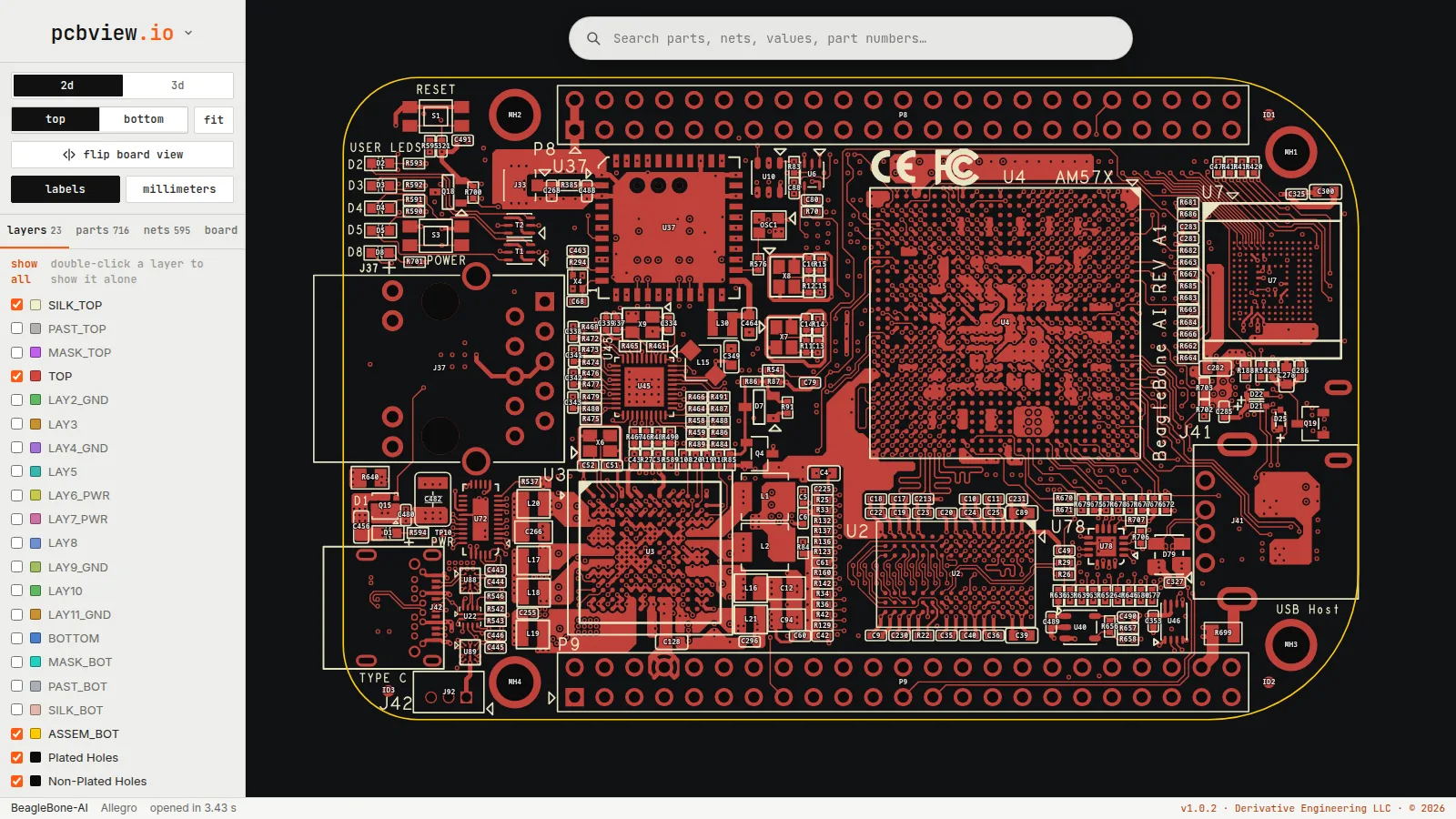
Every homebrewer knows the moment. Someone drops a link to an open source radio board, a filter, an antenna tuner, a QRP transceiver, and the repository holds a zip of Gerbers with cryptic Protel extensions. To actually see the board you’re expected to install a full EDA suite, learn its importer quirks, and wait through a splash screen, all for a two minute question: does this look right, will it fit my enclosure, is that the footprint I think it is. Club mailing lists quietly fill with screenshots taken on someone else’s machine because nobody wants to be the one who installs 4 GB of CAD software to answer a yes or no question.
PCBView.io removes that whole ritual. It’s a free viewer at https://pcbview.io that opens just about any PCB design file directly in the browser: Gerber RS-274X with X2 and X3 attributes, KiCad boards, Altium PcbDoc, Cadence Allegro and OrCAD .brd, Eagle XML, EasyEDA Standard and Pro, ODB++ jobs, PADS ASCII and binary, IPC-2581, and DipTrace, plus Excellon drills, pick and place, BOMs, IPC-D-356 netlists, and plain archives. Everything is parsed locally on your own computer and nothing is uploaded to any server, which is stated twice in the interface itself, once on the landing card and once in the status line after every import. Version 1.0.2 at the time of writing is the work of Derivative Engineering LLC, contactable at [email protected], and it was introduced to the wider electronics community through an EEVblog forum thread by its developer.
Last updated: November 2026. Current release v1.0.2, published 4 November 2026.
TL;DR: PCBView.io is a free browser based PCB design viewer by Derivative Engineering LLC that opens Gerber (X2/X3), KiCad, Altium, Allegro, Eagle, EasyEDA, ODB++, PADS, IPC-2581 and DipTrace files locally in your browser with nothing uploaded. Drop files, a folder, or a GitHub link, or open the built-in BeagleBone AI example, then inspect layers, search parts and nets, read silkscreen text, flip the board, switch mm and mil, render a 3D view, and export PNG images, mechanical STEP models, or shareable board zips. A matching desktop app for Windows, macOS and Linux runs fully offline. It is free to use with optional pay-what-you-like support through Stripe. It isn’t open source software: the web bundle is proprietary to Derivative Engineering LLC.
What PCBView.io Is
PCBView.io is a free browser based PCB design viewer that opens Gerber, KiCad, Altium, Allegro, Eagle, EasyEDA, ODB++, PADS, IPC-2581 and DipTrace board files locally in your computer’s browser, with no uploads, no account, and no EDA installation.
Unpack that sentence and the design philosophy becomes clear. The landing page is a single card that says “import a pcb” with exactly three ways in: open files, open a folder, or paste a GitHub link, plus a one-click example design for anyone who arrived empty handed. Below the buttons sits a row of format pills, Gerber through DipTrace, and a link to the full format list and help. There’s no login wall, no project dashboard, no cloud workspace trying to upsell you. The viewer parses the copper, mask, paste, silkscreen, drills, parts, and nets on your own machine, draws the board in 2D and 3D, and keeps your color choices in the browser. When you want to share what you opened, the app zips the files you supplied into one archive that someone else drops onto the same page. At no point does a board file travel through a company server, which is the feature that makes this tool usable for unreleased commercial work and club designs under NDA as well as open hardware.
Three facts define the project. First, it is format coverage first: ten native board formats plus drills, placement, BOM, netlist, and nested archives, with per-format notes about exactly which versions and quirks are handled. Second, it is privacy architecture rather than privacy policy: the files never leave because the parser runs client side, so there’s no server side promise to audit. Third, it’s a small commercial freeware project, not a community open source one: free to use, pay what you like toward development through Stripe, copyright 2026 Derivative Engineering LLC, with the JavaScript bundle explicitly marked proprietary. That distinction matters and this article states it plainly, because many viewers in this space are genuinely MIT licensed while this one isn’t.
Why a Browser Viewer With No Uploads Matters
To appreciate PCBView.io, start with how board review usually works. The established paths are a desktop Gerber viewer such as Gerbv or KiCad’s GerbView, a manufacturer portal uploader such as a fab’s online quote page, or a full CAD seat. Each path has a cost. Desktop tools need installing and updating per operating system and often understand Gerbers but not native PcbDoc or .brd files. Manufacturer portals understand plenty but require uploading your intellectual property to a third party server, which is unacceptable for client work, contest designs, or anything under NDA. Full CAD seats understand everything but weigh gigabytes and assume you already speak that tool’s dialect.
PCBView.io collapses all three paths into a URL. A club Elmer can review a member’s first KiCad board without installing KiCad. A buyer can check an ODB++ job from a contractor on a Chromebook. A ham staring at a graduated engineer license exam project or a homebrew transceiver fork on GitHub can paste the repo link and see the board in seconds. The GitHub path deserves emphasis: paste a repo, folder, or file URL and the viewer finds the boards inside it, design files, ODB++ jobs, folders of Gerbers, fab zips, and lets you pick which to open, with the files fetched straight from GitHub to the browser. Public repositories only, which is the correct scope for a client side tool with no credentials.
The privacy angle is the load bearing one. Tracespace, the well known open source Gerber renderer behind many portals, also parses client side, and PCBView.io shares that architecture without sharing its license. Nothing uploaded means the tool works identically for an open hardware release and a pre-patent prototype. It also means the viewer keeps working on flaky field internet once loaded, and the desktop builds take the idea to its conclusion by running with the network unplugged entirely.
Every Format It Opens
The format list below is taken from the viewer’s own help text, which is refreshingly specific about versions and rendering compromises instead of claiming universal support.
| Format | Files accepted | What the viewer reads |
|---|---|---|
| Gerber | .gbr, .gtl, .gbl and other Protel names, or any extension | RS-274X, X2 and X3 from any EDA tool. X2 attributes add nets, pins, and parts so copper becomes searchable. X3 component files add position, rotation, value, part number, and footprint per part. Layers are recognized from X2 file functions or file names. |
| KiCad | .kicad_pcb | Board files from KiCad 4 through 10, with parts, values, footprints, nets, pours, per-layer pad stacks, and mask margins. |
| Altium | .PcbDoc | Altium Designer boards: copper, pours, mask, paste, silkscreen with text, mechanical layers, and drills, with parts, parameters, part numbers, and nets. TrueType text is drawn in a stroke font. Parts marked not fitted in a project variant show as fitted, since variants live in the project file. |
| Allegro | .brd | Cadence Allegro and OrCAD PCB Editor boards from Allegro 16 onward, checked against boards saved by 16.3 through 17.5. Each layer is drawn from the board’s own artwork films, showing what Allegro plots: copper with pour fills and negative planes, mask, paste, silkscreen, drawing layers, and drills. Boards saved by Allegro 15 or older need re-saving in a newer Allegro. |
| Eagle | .brd | XML boards from Eagle 6 onward. Eagle stores pours as outlines, so they are filled here by approximation. |
| EasyEDA | .json (Standard), .epro, .epro2, .eprj, project folders (Pro) | EasyEDA Standard and Pro, also known as LCEDA and JLCEDA. Pro 2 and 3 project files from the online editor and desktop client. Reads parts with LCSC and manufacturer part numbers, nets, pours, text, and imported artwork. A loose Pro .epcb board has no footprints, so its parts show without pads. |
| ODB++ | Job folder, .tgz, .zip | ODB++ v7 and v8 jobs from any EDA tool, tested with Altium, Cadence Allegro, Siemens Xpedition and PADS, KiCad, Autodesk Fusion, EasyEDA, and DipTrace. Reads layers, parts with values and part numbers, nets, and drill holes. |
| PADS | .asc, .pcb | PADS Layout and PowerPCB: ASCII .asc from PowerPCB 5 through PADS VX, plus binary .pcb. Reads layers, parts, footprints, nets, tracks, vias, saved pour fills, and text. Part values and attributes come from .asc files. |
| IPC-2581 | .xml, .cvg | Revisions A through C. One file holds the whole board including its BOM. |
| DipTrace | .dip | DipTrace boards from DipTrace 2 through 5 (file formats 37 through 62). Reads layers, parts with values, footprints, nets, tracks, vias, saved pour fills, board text, shapes, and part markings. Silkscreen pictures are not drawn. |
| Excellon drills | .drl, .xln, .txt and others | Drill and route files, plated and non-plated. Altium .txt drills are recognized by content. |
| Pick and place | .csv, .pos, .txt, .mnt and others | Placement files from KiCad, Altium, Eagle, and generic CSV. Units and columns are worked out from the file. |
| BOM | .csv, .tsv, .txt | Comma, tab, or semicolon separated. Matched to parts by reference designator, so search finds values and part numbers. |
| IPC-D-356 netlist | .ipc, .d356, .356 | Bare-board test netlist: net names for pins and test points. |
| Archives | .zip, .tgz, .tar.gz, .tar | Opened in place, with nested archives and folders included. |
Two honest limitations are documented inline and worth repeating. Drill chart symbols on Allegro drawing layers aren’t drawn, and DipTrace silkscreen pictures are skipped. Eagle and EasyEDA pours saved without their fill are approximated rather than exact. These are the normal scars of supporting eleven layout tools without owning any of them, and the viewer discloses each one at the point of use instead of failing silently.
Tour of the Viewer: From Drop to Net Highlight
Opening a board takes seconds. Drop files or a folder onto the page, or click through the buttons, and a status sequence narrates the import: reading files, unpacking archives, identifying board files, merging layers, parts and nets, then drawing the board, with an elapsed-seconds readout in the footer when it finishes. The built-in example is the BeagleBone AI hardware, loaded from its Eagle .brd on GitHub, which opens as a 23-layer, 716-part, 595-net Allegro-class demonstration that immediately shows what the layer panel and search box are for.
The 2D view is the working surface. Toggle between top and bottom copper with one click, mirror the view as if the board were turned over, flip between 2D and flat-shaded 3D, and show or hide reference designator labels. Units switch between millimeters and mils. Each layer gets its own row with color chip and checkbox, double-click or press and hold a layer to isolate it, and plated and non-plated holes get independent toggles. The viewer remembers a sensible default of top copper, top silkscreen, holes, and outline, and a reset control restores it.
Search is the standout interaction. One box covers parts, values, part numbers, nets, and pins, with an optional pass that reads part designators straight from the silkscreen artwork using on-device text recognition. Pick a net and the viewer highlights its copper, lets you widen the selection from the object under the cursor to everything connected on that layer and then on all layers, and reports routed track length per net. If the imported files carry no connectivity, the panel says so directly and tells you what would fix it: Gerber X2 with net attributes, an IPC-D-356 netlist, or a native design file.
Solder mask, silkscreen, and finish colors are adjustable, including ENIG-style gold versus HASL, silver, tin, bare copper, and OSP treatments plus arbitrary mask and silk colors, with a reset to defaults. Colors persist in the browser across boards. Keyboard, mouse, and touch operation are all first class: scroll to zoom, drag to pan, tap to select copper or a part under the finger, tap again to widen, two-finger tap and press-and-hold variants on touch, and a hold-to-preview gesture that shows what sits under the finger without committing to a selection.
3D View, STEP Export, Images, and Sharing
The 3D button renders the board with its solder mask, silkscreen, and finish, extruded to the board thickness with cutouts, slots, and mounting holes. Navigation is orbit style with fit and reset controls. It’s a presentation view rather than a mechanical CAD model, but the export next to it crosses that gap: Save STEP writes a small 3D model for mechanical CAD containing the board at its thickness with cutouts, slots, and mounting holes, plus each part as a box named by its designator. Vias and small pins are omitted, identical parts share one shape definition, and the file never exceeds 5 MB. That is exactly the envelope a 3D-printed enclosure designer or a front-panel layout needs: true outline, true holes, approximate components.
Save image exports a PNG of the current view, which is how the screenshots in this article were produced and how club newsletters get their board illustrations. Save board files collects the files you opened into one zip so the next person drops it onto PCBView.io and sees the same board, with the help text making the privacy point a third time: whoever gets it opens it locally, since nothing goes through a server. Together the three exports cover the three audiences for board review: the forum post (PNG), the enclosure designer (STEP), and the collaborator (zip).
Desktop App: The Same Viewer With the Network Unplugged
PCBView.io also ships as a native-feeling desktop app for Windows, macOS, and Linux, served from the pcbview-releases GitHub repository. The file list is short and conventional: a Windows installer, separate Apple silicon and Intel disk images for macOS, and a Linux AppImage, with Open With integration so Gerbers and board files launch straight into the viewer. Functionally it’s the same viewer, with one stated difference: it runs with the network unplugged, and the only thing it ever asks the internet for is whether a newer version exists.
That offline property is the point. Field laptops, contest stations, and EMC test chambers with no connectivity get the full viewer. The one platform quirk is documented in the help: on macOS the first launch needs the familiar System Settings, Privacy and Security, Open Anyway approval for an unnotarized developer build. Automatic update checks keep the app current without an app store, and the web version needs no install at all.
PCBView.io Against the Usual Viewers
No tool covers every workflow, so here is where PCBView.io sits relative to the viewers hams and homebrewers actually use.
| Viewer | Runs | Native board files | Gerber + drills | 3D / STEP | Privacy model | License and cost |
|---|---|---|---|---|---|---|
| PCBView.io | Browser, plus offline desktop app | KiCad, Altium, Allegro, Eagle, EasyEDA, ODB++, PADS, IPC-2581, DipTrace | Yes, X2/X3 with nets and parts | 3D view plus STEP export under 5 MB | Local parsing, nothing uploaded | Proprietary freeware, free to use, pay what you like |
| KiCad GerbView | Desktop | KiCad native, Gerbers only otherwise | Yes | No 3D board assembly view | Fully local | Open source, free |
| Gerbv | Desktop | No, Gerber and drill only | Yes, RS-274X and Excellon | No | Fully local | Open source, free |
| Tracespace | Browser | No, Gerber focused | Yes, high fidelity SVG render | No | Client side render, nothing uploaded | MIT open source, free |
| Manufacturer portal viewers | Browser | Varies by fab | Yes | Usually 3D render only | Files uploaded to vendor servers | Free with quote flow |
| Altium 365 viewer | Browser | Altium native, best in class | Yes | Yes, full MCAD co-design | Cloud workspace, account required | Commercial, free tier limited |
Read the table as a decision guide. If you need a guaranteed-correct Altium collaboration space with commenting and supply chain data, the vendor cloud still wins. If you need an embeddable MIT licensed renderer inside your own tooling, Tracespace remains the answer. If you need to open one arbitrary board file from the internet in under a minute on a machine you don’t administer, with no account and no upload, PCBView.io is currently the fastest path this author has tested, and the only entry in the table that spans ten native formats plus STEP export from a URL.
Practical Uses in a Ham Shack
The ham radio angle is concrete rather than aspirational, because open hardware is where much of modern ham construction lives. Before sending a forked QRP transceiver, antenna analyzer, or ATU controller to fabrication, open its Gerbers in PCBView.io and check the stackup visually: top and bottom copper present, mask openings where connectors meet the board, paste only where it belongs, silkscreen readable and not buried under pads, and the outline continuous with mounting holes where the enclosure expects them. Isolate the outline layer alone to catch the classic failure of a slot drawn on the wrong layer.
Use the search box as a design review tool. Type a regulator designator and confirm its input and output nets actually reach the bulk capacitors. Highlight a ground net and verify the pour is continuous under the PA stage instead of slot-rotted by thoughtless track routing. Read the pick and place or BOM alongside the layout to confirm the LCSC part number in the EasyEDA project matches the footprint on the board. For kit builders, the silkscreen text reader turns a blurry assembly photo question into a searchable answer: find the designator on the board view first, then locate it on the physical PCB.
The GitHub workflow earns its own paragraph because it matches how open ham hardware is distributed. Many projects link schematics and firmware prominently while the board files sit two folders deep. Pasting the repository URL into PCBView.io surfaces the boards automatically and presents a picker when several revisions are present, which makes comparing a v1.2 layout against the v1.1 you already built a two minute job. Pair that with the shareable zip when asking for help: instead of mailing screenshots back and forth on the club list, send one zip that any member can drop onto the same page and inspect with identical layer settings.
Field and.club contexts benefit most. A laptop at Field Day or a summit with no EDA installed can still open a suspect controller board for inspection using the offline desktop app. A club homebrew night can project one URL and walk twenty members through a real four-layer board, toggling pours and nets live, with no software installation on the venue machine. And for mentors, the combination of net highlighting plus track length readout gives a gentle on-ramp to the two concepts beginners struggle with most: connectivity and return current.
Honest Limits
This section is deliberately blunt, because a viewer earns trust by stating what it can’t do. PCBView.io is free but not open source: the web application is proprietary to Derivative Engineering LLC, so anyone evaluating it for inclusion in a fully open toolchain, a Linux distribution main archive, or a GPL compliance story should treat it as freeware, not FLOSS. That’s a philosophical limit for some shops and a non-issue for others, but it must be explicit.
Technical limits follow from the multi-format ambition. Altium project variants live in the project file, so parts marked not fitted in a variant render as fitted. Eagle and EasyEDA pours saved as outlines are approximated. Boards saved by Allegro 15 or older must be re-saved in a newer Allegro before opening. Drill chart symbols on Allegro drawing layers are skipped, DipTrace silkscreen pictures are skipped, and a loose EasyEDA Pro .epcb board without footprints shows parts without pads. TrueType text throughout is redrawn in stroke fonts, including the Hershey Simplex face credited in the help, so typography-critical silkscreen art may differ subtly from the CAD original.
Operational limits are narrower. GitHub import covers public repositories only, which rules out private client repos unless you download and drop the files manually. The help lists a coming-next section, signaling active development rather than a finished specification, and anyone with a board that refuses to open is asked to mail the developer with the producing tool and version, sending the files only if happy to share them. None of these are disqualifying for review, inspection, and teaching work, but anyone planning production sign-off should keep a native CAD seat in the loop for the final check.
Getting Started in Two Minutes
Open https://pcbview.io in any modern desktop browser. If you have files locally, drag them onto the page or use the open files and open folder buttons; archives including nested zips are unpacked in place. If the design lives on GitHub, paste the repository, folder, or file link into the address-style input instead. With nothing at hand, click the example design link to open the BeagleBone AI board and explore freely. Import settings tucked below the buttons control silkscreen text reading and the default millimeter or mil units, and they apply to the next board opened rather than the current one.
Once the board renders, work through five gestures that cover most reviews. Scroll to zoom and drag to pan, then double-click any layer to isolate it and double-click again to return. Type a part designator or net name into the search box and step through the matches. Click copper to select it, click again to widen to the layer net, and once more for the all-layer net, watching the track length readout. Flip between top and bottom, toggle labels, and finish with the 3D button for a sanity check of component heights against the enclosure. Save a PNG for the build log, a STEP for the mechanical designer, or a zip for the next reviewer, and you are done before any CAD installer would have finished downloading.
Sources and Further Reading
- PCBView.io, the viewer itself: https://pcbview.io/
- EEVblog forum announcement thread: https://www.eevblog.com/forum/eda/pcbview-io-free-browser-based-pcb-design-viewer/
- Desktop app releases (Windows, macOS, Linux): https://github.com/woodruffrb/pcbview-releases
- BeagleBone AI hardware, the built-in example design: https://github.com/beagleboard/beaglebone-ai
- Gerber format specification (Ucamco): https://www.ucamco.com/en/gerber
- IPC-2581 consortium standard: https://www.ipc2581.com
- ODB++Design, Siemens official format site: https://odbplusplus.com/design
- Tracespace open source Gerber renderer: https://tracespace.io
- KiCad EDA, GerbView included: https://www.kicad.org
- Gerbv Gerber viewer (gEDA project): https://gerbv.github.io
- three.js, the 3D rendering library used by the viewer: https://threejs.org
73 de 9M2PJU.



Post Comment